2 ZnO-based Photonic Devices
2.1 ZnO epilayers grown by ALD
High-quality ZnO can be prepared using several techniques, including molecular beam epitaxy (MBE), metal-organic chemical vapor deposition (MOCVD), chemical vapor deposition (CVD), pulsed laser deposition (PLD), and filtered cathodic vacuum arc (FCVA) process, and radio-frequency magnetron sputtering (RFMS). However, the highest ZnO growth rate along the c axis usually results in a columnar morphology in ZnO. The self-limiting characteristics and layer-by-layer growth of ALD indicates that ALD is a noteworthy technique for growing high-quality ZnO thin films.
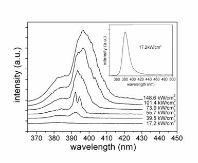
In this study, high-quality ZnO epilayers were grown on (0002)-oriented sapphire substrates by ALD, followed by high-temperature post-deposition annealing and surface passivation by overcoating an ALD Al2O3 layer. The post-annealing treatment improved the crystallinity of the ZnO epilayers and the Al2O3 surface passivation layer effectively suppressed surface nonradiative recombination. X-ray diffraction (XRD) measurement reveals that the ZnO epilayers possessed high crystallinity with c-axis orientation. Photoluminescence (PL) measurements conducted in a backscattering configuration showed that room-temperature stimulated emission associated with exciton-exciton scattering and electron-hole plasma (EHP) in the ZnO epilayer has a threshold as low as 35.1 kW/cm2. This may be attributed to the high-quality ZnO epilayer and Al2O3 surface passivation layer grown by ALD. The result indicate that ZnO epilayers grown by the ALD technique are applicable to next-generation short-wavelength photonic devices.
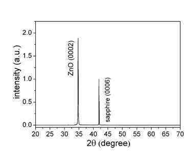
XRD pattern of the post-annealed ZnO epilayer. The appearance of a sharp ZnO (0002) peak reveals that the ZnO epilayer has high crystallinity with c-axis orientation.
Room-temperature PL spectra of the post-annealed ZnO epilayer with the Al2O3 surface passivation layer at various excitation intensities. The inset is the PL spectrum at an excitation intensity of 17.2 kW/cm2. Spectral peak associated with exciton-exciton scattering and EHP appeared in the PL spectra.

The PL intensity as function of the excitation intensity of the post-annealed ZnO films with and without the Al2O3 surface passivation layer. A rapid increase in the PL intensity was clearly seen as the excitation intensity was greater than a threshold value. The significant increase in the PL intensity for the excitation intensity greater than the threshold and the appearance of the spectral peaks demonstrate the occurrence of stimulated emission in the ZnO epilayer.
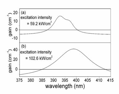
The optical gain spectra of the post-annealed ZnO film with the Al2O3 surface passivation layer at excitation intensities of (a) 59.2 kW/cm2 and (b) 102.6 kW/cm2, measured by the variable stripe length (VSL) technique.
2.2 ZnO quantum dots
ZnO quantum dots are of great interest due to the three-dimensional confinement. It had been reported that the exciton-photon coupling in ZnO quantum dots is particularly strong and the third-order nonlinear susceptibility of ZnO quantum dots is 500 times larger than that of bulk ZnO. However, since ZnO exhibits significant exciton binding energy (~60meV), the Bohr radius of excitons is very small (~1.8 nm). The quantum confinement effects would not occur until the sizes of nanostructures are comparable with the Bohr radius. The small exciton radius of ZnO leads to the difficulty in the observation of the quantum confinement effects in the ZnO nanostructures. Thus the fabrication of ZnO quantum dots is the most challenging among various ZnO nanostructures.
In this study, ZnO quantum dots embedded in the SiO2 layer has been fabricated using the ALD technique. SiO2 nanoparticles with diameters about 10 nm dispersed in isopropyl alcohol solution were spin-on coated on the Si substrate and dried in an oven. Using a unique advantage of ALD which can deposit films with high conformality and good step coverage, ZnO was deposited into the voids between the SiO2 nanoparticles, even in the SiO2 nanoparticle layer as thick as 150 nm or above. It is revealed that the crystallized ZnO quantum dots with diameter in the range of 3~8 nm are uniformly embedded in SiO2 matrix after a high-temperature post-deposition annealing treatment. Quantum confinement effect of the ZnO dots was well manifested by a significant blue-shift about 80 meV in the photoluminescence (PL) spectrum at room temperature. This method can easily prepare ZnO quantum dots embedded in the SiO2 layer with a thickness greater than 100 nm, providing a large active volume for optoelectronic applications.
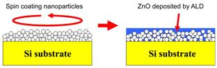
Schema of the fabrication of ZnO quantum dots. ZnO was deposited in voids between SiO2 nanoparticles.
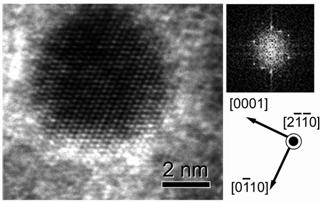
High-resolution (HR) TEM image of the ZnO quantum dots embedded in the SiO2 layer.
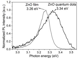
Normalized PL spectra of the ZnO quantum dots embedded in the SiO2 layer and the ZnO thin film at room temperature, indicating a remarkable blue-shift about 80 meV of the ZnO quantum dots.
2.3 ZnO-based Ultraviolet Light-emitting Diodes
(2.3.1) n-ZnO/p-GaN Heterojunction LEDs
Although ZnO technology has considerably been progressing recently, it is still difficult to prepare reproducible and stable p-type ZnO films with high carrier concentration and low resistivity. Since ZnO and GaN have the same crystal structure (wurtzite) with a small in-plane lattice mismatch (1.8%), p-type GaN would be substituted for the p-ZnO. In this study, ALD technique and subsequent rapid thermal annealing (RTA) were implemented to grow high-quality ZnO epilayers for the fabrication of n-ZnO/p-GaN heterojunction light-emitting diodes (LEDs). The X-ray diffraction measurement reveals that the ZnO epilayer has high crystallinity with c axis orientation. Transmission electron microscopy (TEM) images reveal that the ZnO grows in good epitaxial relation with GaN and to almost a perfect single crystal with a very few dislocations. It has been found that the threading dislocations from the underlying layers reduce at the interface between GaN and ZnO, due to the layer-by-layer growth of ALD and the recrystallization during the post heat treatment of RTA. Room temperature ultraviolet electroluminescence (EL) at 391 nm from ZnO was achieved at a low injection current about 10 mA. It is concluded that the competition between the ELs from the n-ZnO and p-GaN (λ~425 nm) may be ascribed to the ZnO/GaN interface states coupled with the differences between the n-ZnO and p-GaN in carrier concentration and light emission efficiency. The achievement of UV EL at a low DC injection current from ZnO indicates that the ZnO epilayers grown by the ALD technique are effectually applicable to the next-generation short-wavelength photonic devices.
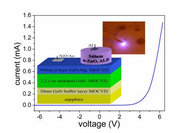
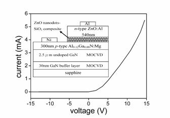
Current vs. voltage (I-V) curve of the n-ZnO/p-GaN heterojunction LED. The insets show the device structure and the EL image.
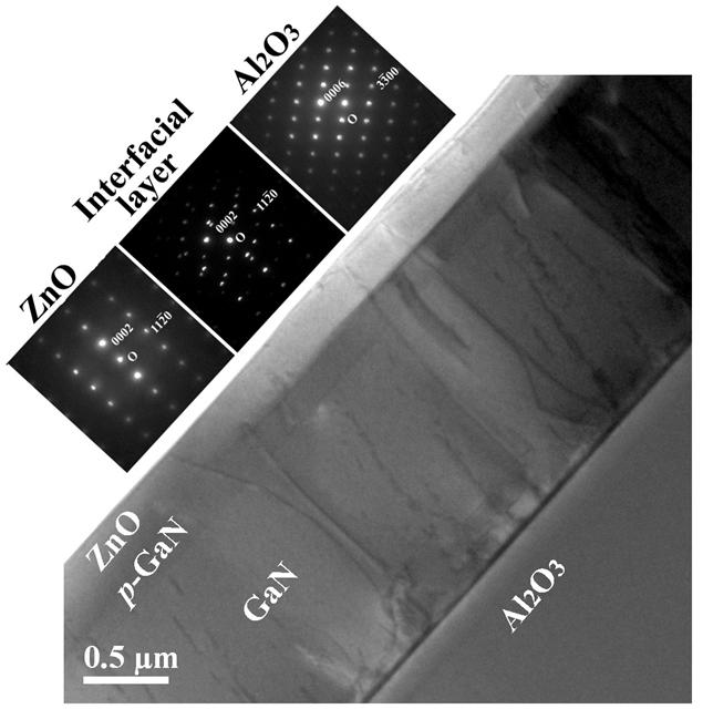
Cross-sectional bright-field TEM image of the n-ZnO/p-GaN heterojunction on the underlying GaN and Al2O3 substrate, and selected-area electron diffraction patterns from the Al2O3 layer, the interfacial layer and the ZnO layer. The spots in the interfacial layer comprise the spots from the ZnO (whose 0002 and 110 spots are marked) and additional spots from an unknown crystal formed with an orientation with their c-axis.
(2.3.2) n-ZnO/ZnO nanodots-SiO2 composite/p-AlGaN heterojunction LEDs
This study demonstrates amplified spontaneous emission (ASE) of the ultraviolet (UV) electroluminescence (EL) from ZnO at λ~380 nm in the n-ZnO/ZnO nanodots-SiO2 composite/p-Al0.12Ga0.88N heterojunction LEDs. A SiO2 layer embedded with ZnO nanodots was prepared on the p-type Al0.12Ga0.88N using spin-on coating of SiO2 nanoparticles followed by ALD of ZnO. An n-type Al-doped ZnO layer was deposited upon the ZnO nanodots-SiO2 composite layer also by the ALD technique. The ZnO nanodots embedded in the SiO2 matrix allows the transport of carriers through the thick ZnO nanodots-SiO2 composite layer. The high quality of the n-ZnO layer was manifested by the well crystallized lattice image in the HRTEM picture and the low-threshold optically pumped stimulated emission. The low refractive index of the ZnO nanodots-SiO2 composite layer (n~1.52) contributes to (1) the increase in the light extraction efficiency from n-ZnO, (2) the low-threshold optically pumped stimulated emission in n-ZnO, and (3) the internal optical feedback of UV EL back into the n-ZnO layer. Consequently, significant enhancement of the UV EL intensity and super-linear increase in the EL intensity, as well as the spectral narrowing, with injection current were observed owing to ASE in the n-ZnO layer.
Current vs. voltage (I-V) curve of the n-ZnO/ZnO nanodots-SiO2 composite/ p-Al0.12Ga0.88N heterojunction LED at room temperature. The inset is the schematic diagram of the device structure.
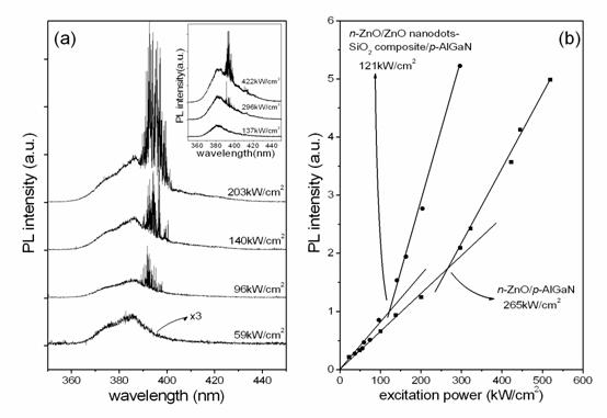
(a) Room-temperature PL spectra of the n-ZnO layer in the n-ZnO/ZnO nanodots-SiO2 composite/p-Al0.12Ga0.88N structure pumped by a fourth harmonic Q-switched Nd:YAG laser at various excitation intensities. Inset shows the PL spectra of the n-ZnO layer in the n-ZnO/p-Al0.12Ga0.88N structure at room temperature. The appearance of the narrow spectral peaks may come from the constructive closed-loop paths via the multiple scattering between the optical scattering centers and crystalline grains in the n-ZnO layer.
(b) PL intensity as function of the excitation intensity of the n-ZnO layers in the n-ZnO/ZnO nanodots-SiO2 composite/p-Al0.12Ga0.88N and n-ZnO/p-Al0.12Ga0.88N structures at room temperature. The appearance of the spectral peaks coupled with the significant increase in the PL intensity for the excitation intensity greater than the threshold indicate that the occurrence of stimulated emission in the n-ZnO layers.
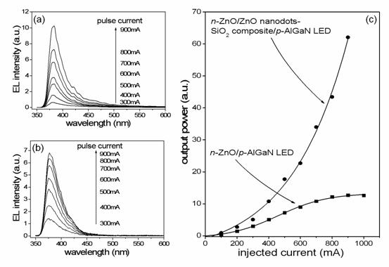
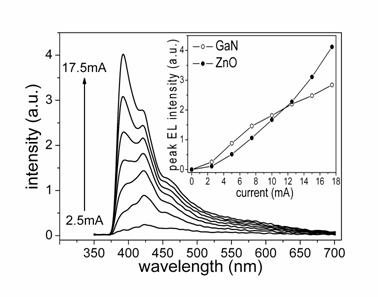
(a) Room-temperature EL spectra of the n-ZnO/ZnO nanodots-SiO2 composite/p- Al0.12Ga0.88N heterojunction LED under the injection of various pulse currents. (b) Room-temperature EL spectra of the n-ZnO/p-Al0.12Ga0.88N heterojunction LED under the injection of various pulse currents. (c) Relationships between the EL intensity and the injection current of the n-ZnO/ZnO nanodots-SiO2 composite/p-Al0.12Ga0.88N and n-ZnO/p-Al0.12Ga0.88N heterojunction LEDs at room temperature. It can be seen clearly that the EL intensity increases only linearly with the injection current and saturates at high injection current for the n-ZnO/p-Al0.12Ga0.88N LED. On the other hand, significant enhancement of the EL intensity and super-linear increase in EL intensity with the injection current were observed for the device with a ZnO nanodots-SiO2 composite layer inserted between the n-ZnO and p-Al0.2Ga0.8N layers.
(2.3.3) n-ZnO/i-ZnO/p-SiC heterojunction LEDs
A major obstacle in the development of ZnO LEDs is the difficulty of fabricating high-quality and reproducible p-type ZnO with high carrier concentration. As a result, growing high-quality n-type ZnO films on good lattice-matching p-type substrates to form heterojunction LEDs is an alternative approach to overcoming this problem. GaN has been considered a good candidate for the p-type substrate and several groups have fabricated the n-ZnO/p-GaN heterojunction LEDs. Commercially available 4H-SiC is also a good p-type substrate candidate for ZnO-based heterojunction LEDs because of the same crystal structure (wurtzite) and a small in-plane lattice mismatch (~5%) with ZnO. In this study, ALD was used to grow n-type Al-doped ZnO (n-ZnO) and undoped ZnO (i-ZnO) layers on p-type 4H-SiC substrates, to fabricate n-ZnO/p-SiC and n-ZnO/i-ZnO/p-SiC heterojunction light-emitting diodes (LEDs). For the n-ZnO/p-SiC LED, since the electron injection from n-ZnO into p-SiC has a smaller energy barrier than the hole injection from p-SiC into n-ZnO, the light emission mainly originated from p-SiC broad defect-related bands. The i-ZnO layer with a low electron concentration in the n-ZnO/i-ZnO/p-SiC structure leads to the injection of electrons from n-ZnO and holes from p-SiC into the i-ZnO layer to produce UV EL, coupled with a decrease in the electron injection from ZnO into SiC. Significant and dominant UV EL from ZnO was thus achieved in the n-ZnO/i-ZnO/p-SiC heterojunction LED.